Originally published on Laser Focus World?
炬光科技多年來一直注重基礎(chǔ)研究,每年在專業(yè)期刊、雜志、學(xué)術(shù)會議等平臺發(fā)表各類技術(shù)文章,并曾出版世界第一本高功率半導(dǎo)體激光器封裝專著。近日,《Laser Focus World》發(fā)表了炬光科技首席科學(xué)家王警衛(wèi)等撰寫的技術(shù)文章《Simulation and modeling play key roles in high-power diode-laser packaging》,文章針對激光技術(shù)發(fā)展對封裝技術(shù)提出的新挑戰(zhàn),介紹了仿真和建模在高功率半導(dǎo)體激光器封裝中發(fā)揮的關(guān)鍵作用。
文章概要如下:
高功率半導(dǎo)體激光器已廣泛應(yīng)用于很多行業(yè)。隨著激光技術(shù)的發(fā)展,其輸出光功率越來越高,激光巴條的腔長也相應(yīng)地由1mm增加到了4mm。因此,巴條的廢熱能量密度從200W/cm2急劇增加到>600W/cm2。為獲得低的“SMILE”,如<1μm,或防止巴條在貼片鍵合后出現(xiàn)裂紋,需要采用腔長1.5mm~4mm的巴條,并優(yōu)化封裝結(jié)構(gòu),最大限度地降低熱應(yīng)力。這兩者都給現(xiàn)有的封裝技術(shù)帶來了挑戰(zhàn),從而有必要使用有限元模型(FEM)來計算和模擬高功率半導(dǎo)體激光器的熱行為和熱應(yīng)力管理。
我們研究了在連續(xù)波(CW)或準(zhǔn)連續(xù)波(QCW)模式下,不同封裝結(jié)構(gòu)有限元模擬技術(shù)的應(yīng)用,所涉及的計算和模擬仿真都是基于炬光科技的產(chǎn)品,包括單巴傳導(dǎo)冷卻/微通道系列、傳導(dǎo)冷卻G-stack、水冷疊陣和面陣。我們還提出了在制造高功率半導(dǎo)體激光器之前利用FEM工具進(jìn)行熱與應(yīng)力模擬的指導(dǎo)方針。此類模擬仿真結(jié)果可有效降低封裝結(jié)構(gòu)或激光系統(tǒng)出現(xiàn)的潛在熱與應(yīng)力風(fēng)險,并有助于降低試驗(yàn)成本、優(yōu)化流程,最終滿足不同客戶的需求。
Simulation and modeling play key roles in high-power diode-laser packaging
Finite-element method (FEM) simulations reduce potential thermal and stress risks when designing packaging structures for high-power laser-diodes.
JINGWEI WANG, TUANWEI FU, and XUEJIE LIANG
FOCUSLIGHT TECHNOLOGIES INC.
High-power diode-lasers (HPDLs) are now widely used for industrial (materials processing procedures such as welding, cutting, surface treatment, etc.), scientific, and medical applications. The need to design advanced high-power laser packages, to understand the physics of the behaviors of these packages and its interfaces, and to prevent possible functional (optical) and mechanical (physical) failures are of obvious practical importance. As laser technologies develop, the output power of HPDLs has grown, along with the cavity length of diode laser bars increasing from 1 to 4 mm. As a result, the waste-heat energy density of a single diode laser bar has increased dramatically from 200 W/cm2 to more than 600 W/cm2.
Many failures in HPDLs—for example, bonding interfaces—are directly related to the packaging.1 Thermal behaviors of the bonding interfaces and thermal stresses between the bonding interfaces are the major factors affecting the functional and structural performance of HPDLs. If the accumulated heat cannot readily escape, the elevated temperature and thermally induced stress at the location of the p-n junction will not only adversely affect the output power, slope efficiency, threshold current, and device lifetime, but could also cause spectral broadening and wavelength shifts.2 The emitting wavelengths will shift if the junction temperature of the emitters across the array is not well controlled and/or not uniform. The above-mentioned scenarios make the thermal management of high-power laser devices a major challenge in designing, manufacturing, and utilizing HPDLs.
Simulation and modeling of thermal stress in packaging of HPDLs
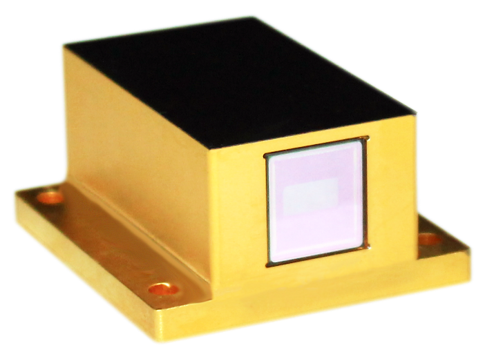
FIGURE 1. An AL01 1064 nm laser module for lidar. (Courtesy of Focuslight)
Automotive lidar has become a very popular application for lasers in recent years. Focuslight Technologies (X’ian, China) offers various products for automotive lidar applications. Focuslight’s AL01 laser module (see Fig. 1) is designed for flash lidar applications. The module is a diode-pumped solid-state (DPSS) laser that uses Q-switch technology to enable pulse energies of up to 1.5 mJ per 3 ns pulse at 1064 nm wavelength. To ensure its stability at automotive-grade temperatures (-40° to 80°C), the module was designed and manufactured with advanced bonding and assembly processes; some special materials have been used as well.
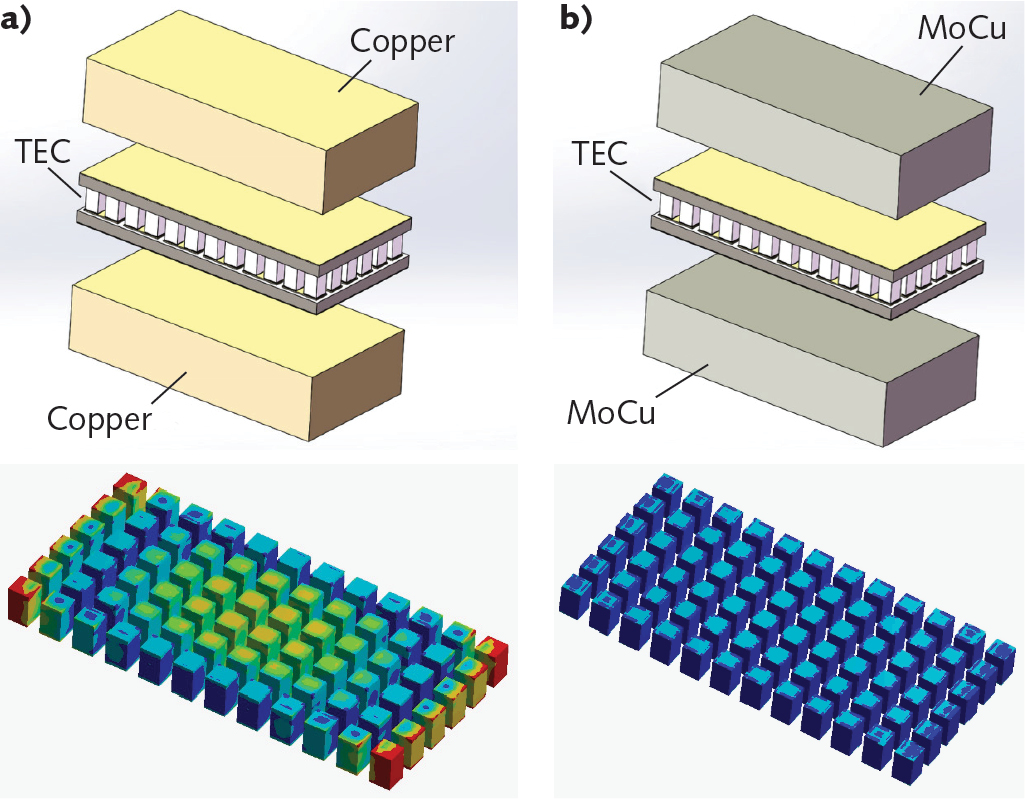
FIGURE 2. Structure and stress: mismatched CTE (a) and matched CTE (b).
During the design process, the coefficient of thermal expansion (CTE)-matched principle was taken into account as a crucial factor. CTE mismatch between the laser bar and the thermoelectric cooler (TEC) could bring large thermal stress to the packaging process, cause a lot of cracks at the corner of the TEC, and potentially lead to device failure. The optimized selection of materials and dimensions has been achieved through repeated calculation and simulation modeling (see Fig. 2). By doing this, the final packaging structure has prevented cracks from forming at the corner of the TEC. Digital simulations helped the developer to find the right solution rapidly. Mass production and stable performance of AL01 modules have proved that the package design is optimal.
Industrial applications. Kilowatt- or even hundred-kilowatt-level HPDL stacks are widely used for scientific and industrial applications (such as annealing, bonding, surface treatment, and others). A good example is Focuslight’s 6 kW DLight Series product. Applications such as solid-state laser pumping and materials processing require good beam quality from the diode-laser stack. The near-field nonlinearity along the laser bar (also known as “SMILE”), or the slight bend of the horizontal line connecting the emitters in the bar, is the main obstacle to achieving good beam quality. Minimizing the SMILE of HPDLs is key to achieving high brightness along the fast axis.
Thermal stress causes mechanical strain in the diode and changes the band structure, thus changing the characteristics of the diode laser with respect to threshold, wavelength, polarization, and SMILE. In addition, induced thermal stress in the laser device may cause damage to the laser chips/bars and consequently shorten lifetime of the device.
SMILE and stress controlling.3 The thermal stress affecting the performance and reliability of HPDLs is mainly caused by the CTE mismatch between the mounting substrate and laser chip. For HPDL packaging, packaging materials with high thermal conductivities and CTEs that match those of the semiconductor materials—such as gallium arsenide (GaAs), indium phosphide (InP), and gallium nitride (GaN)—are desired. Thermal-stress management is one of the most critical challenges to packaging of HPDLs.
The bonding of diode laser chips onto their heat sinks is the most important step in the packaging process. Mechanical stress generated in the bonding process has typically always caused chip deformation (SMILE) as the device cooled down from the solder melting point to room temperature. As a result, how to decrease the mechanical stress in the packaging process becomes the key to minimizing the SMILE value.
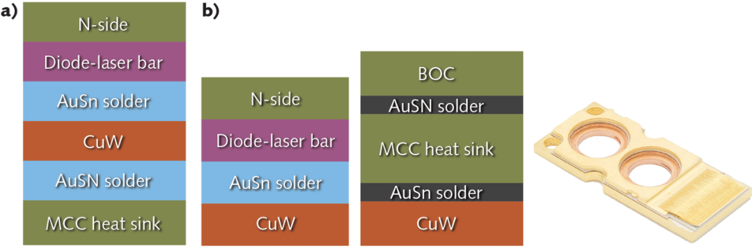
FIGURE 3. Two different laser-diode packaging structures: HMCC (a) and DMCC (b).
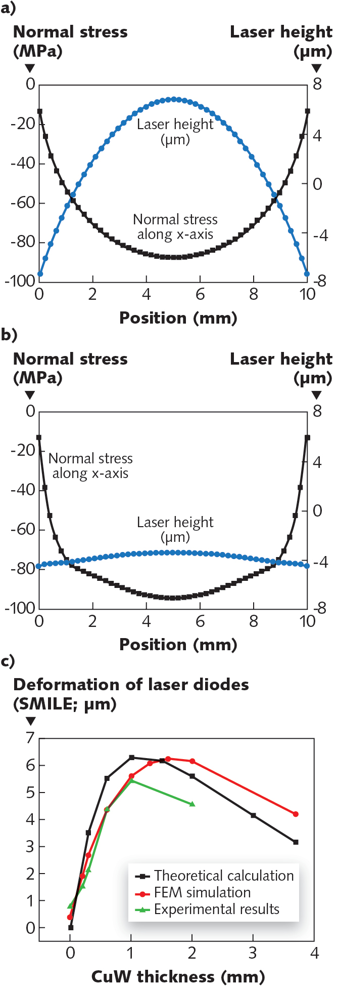
FIGURE 4. Simulation and experiment results: simulated stress of HMCC (a); simulated stress of DMCC (b); and experimental SMILE value with increasing CuW thickness (c).
For digital-simulation modeling of this process, different packaging structures and materials were selected (see Fig. 3); the simulated results are shown in Figure 4a and 4b. A continuous-wave (CW) 200 W diode-laser bar with a thermal density of greater than 500 W/cm2 can be bonded on a microchannel cooler (MCC) heat sink. Thermal-dissipation capability should be considered in the simulation, as well as how to minimize the “SMILE” value. The finite-element model (FEM) simulation results show that the compression stress on the laser bar decreases with the increase of copper-tungsten (CuW) submount thickness, as the CuW submount works as a buffer layer and can thus absorb stress. However, the laser bar out-of-plane strain (SMILE value) is approximately zero when the diode-laser array is directly bonded onto the heat sink without a submount; the SMILE value is maximized when the thickness of the CuW submount is increased to 44% of the heat sink. Beyond this point, the SMILE value decreases with increasing CuW submount thickness. As seen in Figure 4c, the experimental results are well aligned with the simulation results.2 Therefore, the thickness of the submount affects the near-field nonlinearity of a laser bar significantly.
Simulation and modeling of heat in packaging of HPDLs
Scientific applications. Besides the SMILE, spectral width is also one of the key parameters of a diode-laser vertical stack. Improving the stack’s spectral performance is very important for increasing production yield, reducing costs, and enhancing competitiveness. For some scientific applications, narrow spectral width is especially important.
Thermal design of HPDLs is critical, as a rise of junction temperature at the location of the p-n junction will adversely affect the output power, slope efficiency, threshold current, and lifetime of the device if the accumulated heat cannot be easily dissipated. Excessive heat can also cause spectral broadening and wavelength shift. Thermal management of HPDL devices has become a major challenge in laser design, manufacturing, and application.
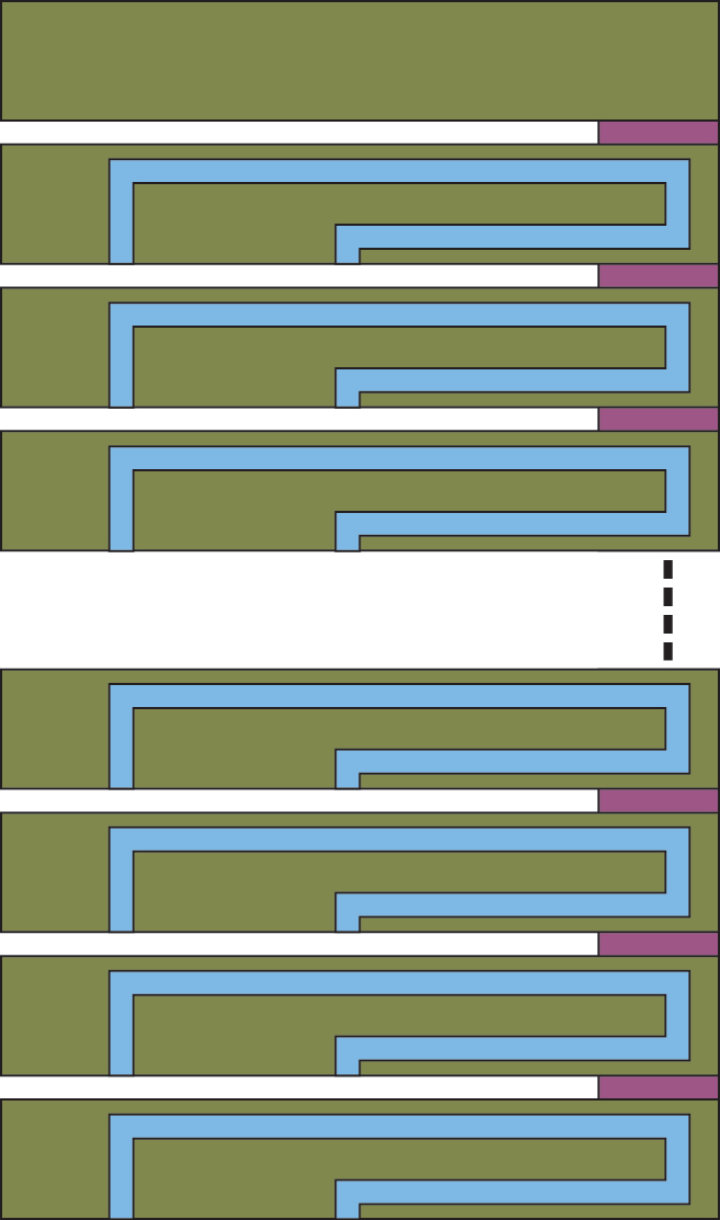
FIGURE 5. Design of parallel format for liquid cooling.
In the design process for a vertical-stack laser, one of the main problems is the thermal crosstalk, which seriously affects the cooling efficiency. To avoid thermal crosstalk, a parallel liquid-cooling format is designed to overcome heat unevenness between the bars, effectively improving the thermal dissipation. Figure 5 shows the design of the parallel format of liquid cooling.
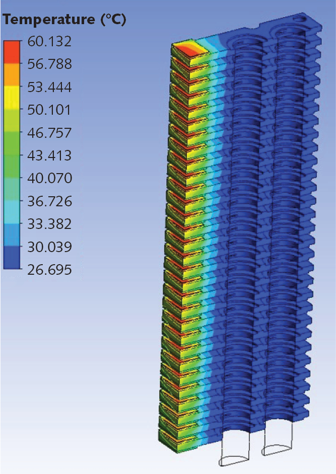
FIGURE 6. Thermal distribution of a MCC-based sack in CW mode.
In the following case, the thermal design and structure optimization of a vertical-stack laser with more than 20 bars was simulated. The simulation results in Figure 6 show that most of the heat is dissipated via the cooling-flow liquid. There is no significant accumulation of heat and the temperature gradient of each bar is relatively uniform. The maximum temperature on the stack is 60.13°C.
Based on the thermal simulation, the structure is optimized in many aspects, such as cooling-water flow rate, microchannel cooler design, and water distribution. The heat is taken away as quickly as possible by the cooling water, ensuring that no thermal accumulation exists between the bars.
Although the laser bars in vertical stacks are simultaneously conduction cooled and microchannel-liquid cooled, temperature nonuniformity remains among the bars due to thermal crosstalk and/or liquid flow nonuniformity. This nonuniformity can alter the wavelength of the bars and broaden the spectrum of the stacks.
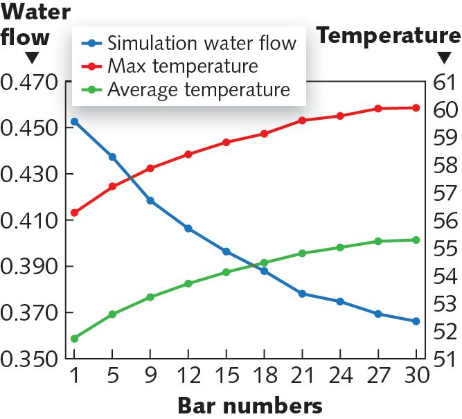
FIGURE 7. Relationship between water flow and temperature.
To achieve a very narrow spectral width, in our work, advanced packaging processes have been used to maintain uniformity of temperature distribution. First, total temperature distribution is simulated and calculated (see Fig. 7). Next, the wavelength of each bar is selected to match the temperature distribution based on the simulation results. The third and last step is to use optimized packaging technology to achieve the same output wavelength. Using this method, the spectrum broadening of a vertical stack can be effectively controlled.
Simulation and modeling of heat and stress in optical collimation microlenses
Optical collimation microlenses, including fast-axis collimators (FACs), slow-axis collimator (SAC) arrays, homogenizers, diffusers, collimators, beam transformation systems (BTS), and so on, are widely used in DPSS lasers, materials processing, 3D sensing, immersive photolithography, flexible display, lidar, and other application fields. These microlenses are commonly fixed on mechanical frames by adhesives. Controlling the stress on lenses and reduce the risk of cracks is therefore of great importance.
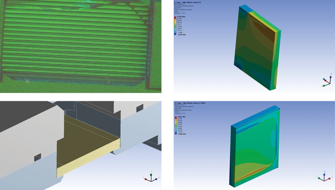
FIGURE 8. Stress optimization on adhesion layer.
A typical example is shown in Figure 8. A disastrous crack is found on a diffuser, although the adhesion is good. Simulation was carried out to look for causes of such cracks; the simulation results show that a higher stress, up to 61.58 MPa, occurred at one corner of the diffuser, which corresponds to the actual crack. After the adhesion in the FEA model was precisely controlled and the program run again, the stress on the diffuser decreased to 32.96 MPa, as shown in the figure. The result shows the benefit of FEM in improving adhesion processes.
Easy-to-use FEM methods have been presented for evaluating the thermal performance of HPDLs and the stress distribution in HPDLs. These methods make it much easier to understand the physics of the addressed thermal phenomena and predict their thermal behavior and performance. Digital-simulation modeling should be conducted before the manufacturing of HPDLs, helping to reduce R&D costs and quickly guiding engineers to the correct approach if thermal and stress distributions in a package are taken into account. The methodology described here for the application of diode-laser packages can also be used beyond this area of engineering for the analysis and design of packaging structures.
ACKNOWLEDGEMENT
DLight is a registered trademark of Focuslight Technologies.
REFERENCES
1. X. Liu et al., J. Appl. Phys., 100, 1, 013104 (2006).
2. H. Zhang et al., “High power 250 W CW conductively cooled diode laser arrays with low SMILE,” Proc. SPIE, 11261, 112610C (Feb. 2020).
3. C. Zah et al., “Low SMILE vertically stacked laser bars enable kW modular line lasers,” High Power Diode Lasers and System Conf. (Coventry, England), 9-10 (2017); doi:10.1109/hpd.2017.8261079.
Jingwei Wang is Chief Scientist, Tuanwei Fu is CAE Engineer, and Xuejie Liang is Manager of the Design and Simulation Technology Department, all at Focuslight Technologies, Xi’an, China.
E-mails: wangjw@focuslight.com, futw@focuslight.com, and liangxj@focuslight.com; www.ruidelawyer.com.
關(guān)于炬光科技:
西安炬光科技股份有限公司成立于2007年,是一家全球領(lǐng)先的專業(yè)從事高功率半導(dǎo)體激光器、激光微光學(xué)元器件、光子技術(shù)應(yīng)用解決方案的研發(fā)、生產(chǎn)及銷售的國家級高新技術(shù)企業(yè)。公司圍繞光子技術(shù)及應(yīng)用領(lǐng)域,致力于為全球客戶提供高功率半導(dǎo)體激光器與激光微光學(xué)核心元器件及光子技術(shù)應(yīng)用解決方案,形成了全面、完善的研發(fā)、生產(chǎn)及銷售服務(wù)體系。


 返回
返回